NOT, OR and AND Gates: Evolution, Truth Tables and a Worked Circuit
Learn how NOT, OR and AND gates developed from switching ideas, then trace F=(A+B')C node by node and confirm it with a complete truth table.
KnowledgeGate Team
Exam prep & CS education
Updated 23 Oct 20265 min read
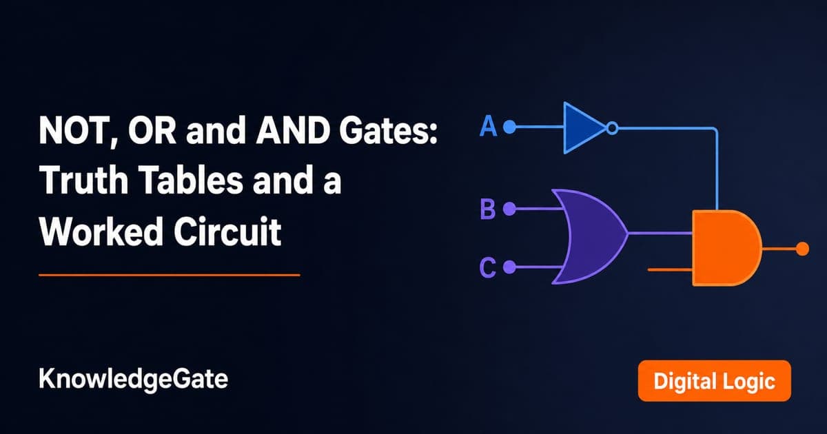
NOT, OR and AND gates are simple when you study each symbol alone. The difficulty begins when a signal is inverted before entering another gate, because one missed bubble changes every later value. The gates' switching origin, symbols, truth tables and Boolean notation lead to one exact three-input circuit. A full truth table checks the result by a second method and exposes any mistake in the node-by-node trace.
Logic gate evolution: from physical switches to Boolean decisions
Switching hardware evolved from electromechanical relays through vacuum-tube and transistor switches to integrated logic. The physical devices changed, but the abstract truth functions AND, OR and NOT stayed the same. A logic gate is a circuit that maps one or more binary inputs to a binary output according to a truth table.
Two normally open switches in series conduct only when both are closed, which models AND. Two switches in parallel conduct when either path is closed, which models inclusive OR. An inverting stage maps a low logical input to a high output and a high input to a low output, which models NOT. Open and closed, or low and high, are useful models for the function, not fixed voltage specifications.
In Boolean notation, + means OR, adjacency or . means AND, and an apostrophe means complement. The values 0 and 1 are logical states, not universal voltage values. Keep a gate's permanent truth rule separate from temporary input values. These ideas sit within the wider CS Fundamentals route.
NOT gate: one input and the complement operation
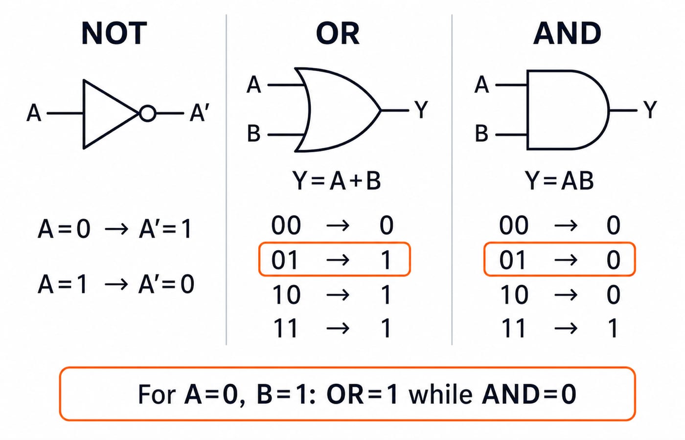
A NOT gate has one input and produces its complement: Y=A'. The small circle on its output is the inversion bubble.
A | Y=A' |
|---|---|
0 | 1 |
1 | 0 |
For the input sequence A: 0, 0, 1, 0, 1, complement each value in place:
0becomes1.0becomes1.1becomes0.0becomes1.1becomes0.
Therefore, Y: 1, 1, 0, 1, 0. Apply a second NOT gate and (A')'=A, restoring 0, 0, 1, 0, 1.
Scope matters. A'B means complement A, then AND it with B; (AB)' complements the whole AND output. At A=0, B=1, both expressions happen to equal 1. At A=1, B=0, however, A'B=0 while (AB)'=1. One counterexample proves that the expressions are not equivalent.
OR and AND gates: two-input truth tables side by side
Inclusive OR is Y=A+B, so its output is 1 when at least one input is 1. AND is Y=AB, so its output is 1 only when both inputs are 1.
A | B | A+B | AB |
|---|---|---|---|
0 | 0 | 0 | 0 |
0 | 1 | 1 | 0 |
1 | 0 | 1 | 0 |
1 | 1 | 1 | 1 |
The mixed rows 01 and 10 diagnose the difference: OR gives 1, while AND gives 0. At 00 both give 0, and at 11 both give 1, so equal-input rows alone cannot identify the gate.
The same rules extend to more inputs. For (A,B,C)=(1,0,0), A+B+C=1 but ABC=0. For (1,1,1), both expressions equal 1. OR here is inclusive OR, not XOR.
Worked circuit: evaluate F=(A+B')C one gate at a time
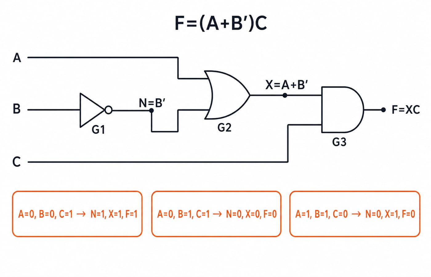
The circuit has inputs A, B and C. Gate G1 inverts B, creating node N=B'. Gate G2 ORs A and N, creating X=A+N=A+B'. Gate G3 ANDs X with C, giving F=XC=(A+B')C. Label N and X before calculating F.
Trace (A,B,C)=(0,0,1) without skipping a node:
N=B'=1.X=A+N=0+1=1.F=XC=1.1=1.
Now change only B and trace (0,1,1): N=0, X=0+0=0, and F=0.1=0. The changed NOT output affects the complete path.
The final AND gate also matters. At (1,1,0), N=0 and X=1, but F=1.0=0. At (1,1,1), the same N=0 and X=1 produce F=1.1=1. A high intermediate node does not guarantee a high final output.
Truth-table verification and an equivalent AND-OR form
A complete truth table checks every input vector.
A | B | C | B' | X=A+B' | F=XC | AC+B'C |
|---|---|---|---|---|---|---|
0 | 0 | 0 | 1 | 1 | 0 | 0 |
0 | 0 | 1 | 1 | 1 | 1 | 1 |
0 | 1 | 0 | 0 | 0 | 0 | 0 |
0 | 1 | 1 | 0 | 0 | 0 | 0 |
1 | 0 | 0 | 1 | 1 | 0 | 0 |
1 | 0 | 1 | 1 | 1 | 1 | 1 |
1 | 1 | 0 | 0 | 1 | 0 | 0 |
1 | 1 | 1 | 0 | 1 | 1 | 1 |
Distribute C across the bracket:
F=(A+B')C=AC+B'C
The final columns agree on all eight rows, so the original NOT-OR-AND circuit and equivalent two-AND-one-OR circuit implement the same function. With A as the most significant bit, the output is 1 for 001, 101 and 111. Therefore, F=Σm(1,5,7).
Use F=(A+B')C when the goal is clean node tracing through NOT, OR and AND. For all seven gate functions, K-map minimisation, universal-gate reconstruction and hardware delay, continue with Logic Gates in Digital Electronics. The Boolean Algebra and K-map Minimization Guide develops the next methods for proving and simplifying larger expressions.
Common NOT, OR and AND gate traps
Boolean + is OR, not ordinary addition, so 1+1=1. OR is also different from XOR: when A=B=1, OR gives 1, while XOR gives 0.
Parentheses and inversion bubbles can change the entire function. At A=0,B=1, A'+B=1, but (A+B)'=0. At A=1,B=1,C=0, A+B'C=1, but (A+B')C=0. These input assignments disprove the respective equivalences.
Use a fixed correction routine:
Mark every inversion first.
Label every intermediate node.
Evaluate complement before AND before OR, unless parentheses override that order.
Verify a claimed equivalence on all rows when there are only two or three variables.
One convenient input can disprove equivalence, but it cannot prove equivalence.
How exams test NOT, OR and AND gates
Typical questions ask you to complete a truth table, identify a gate from input-output rows, find an output for a given input vector, translate a diagram into a Boolean expression, draw a circuit from an expression, match equivalent circuits, or track the effect of an inversion bubble.
Use this rapid check before moving on:
NOT applied to
0,1,1,0gives1,0,0,1.For
A=0,B=1, OR is1and AND is0.For the worked circuit at
A=1,B=0,C=1,B'=1,X=1andF=1.For
AC+B'CatA=0,B=0,C=1, the result is1.
Practise each of these question shapes until you can produce the answer without redrawing the circuit. The GATE Test Series provides a route for timed, exam-style practice after you can solve the circuit by hand.
NOT, OR and AND gates: the short version and next step
NOT flips one bit.
OR needs at least one input to be
1.AND needs every input to be
1.Label intermediate nodes before evaluating the output.
Verify a small circuit with its full truth table.
For this circuit, (A+B')C=AC+B'C, and the output sequence in binary row order is 0,1,0,0,0,1,0,1.
Redraw the circuit from the equation, rebuild the eight-row table without looking, and check the rows 001, 101 and 111, where F=1. If you want Digital Logic placed inside a broader preparation sequence, GATE Guidance by Sanchit Sir is the structured next route.
Keep learning
Binary Arithmetic Operations Explained: Rules and Worked Examples
Learn binary addition, subtraction, multiplication and division with aligned worked examples, then separate carry, borrow and two's-complement overflow.
Updated 19 Oct 20266 min readDigital Logic

1's Complement Explained: Binary Conversion, Addition and Worked Examples
Learn how fixed-width 1's complement numbers represent negatives, why zero has two encodings, and how end-around carry works through exact examples.
Updated 15 Oct 20266 min readDigital Logic
Decimal Conversion Explained: Binary, Octal and Hexadecimal Worked Examples
Learn one dependable method for converting values between decimal, binary, octal and hexadecimal, including fractions, shortcuts and checks.
Updated 11 Oct 20265 min readDigital Logic

Two's Complement Arithmetic Explained: Signed Ranges, Subtraction, Overflow and Worked Examples
Build a reliable 8-bit method for encoding signed values, subtracting with complements, detecting overflow, extending signs and checking every result.
Updated 7 Oct 20266 min readDigital Logic