Shift Registers Explained: Types, Timing and a 4-Bit Worked Trace
Learn one reliable method for tracing shift registers. Fix the bit order, apply simultaneous next-state equations, and follow a complete four-clock example.
KnowledgeGate Team
Exam prep & CS education
Updated 4 Sep 20266 min read
You may know that a register stores bits and still lose track of which bit moves where at a clock edge. Two habits cause most errors: saying left or right without fixing the written bit order, and updating stages one by one instead of together. With four D flip-flops, the same next-state method handles a four-clock trace, distinguishes SISO, SIPO, PISO and PIPO, and answers common exam checks.
Related reading: Shift register MCQs and Flip-flops.
Shift register in one precise mental model
A shift register is a chain of clocked flip-flops. It stores an n-bit state and moves data by one stage on each active clock edge. The four-stage example uses rising-edge D flip-flops connected to the same clock.
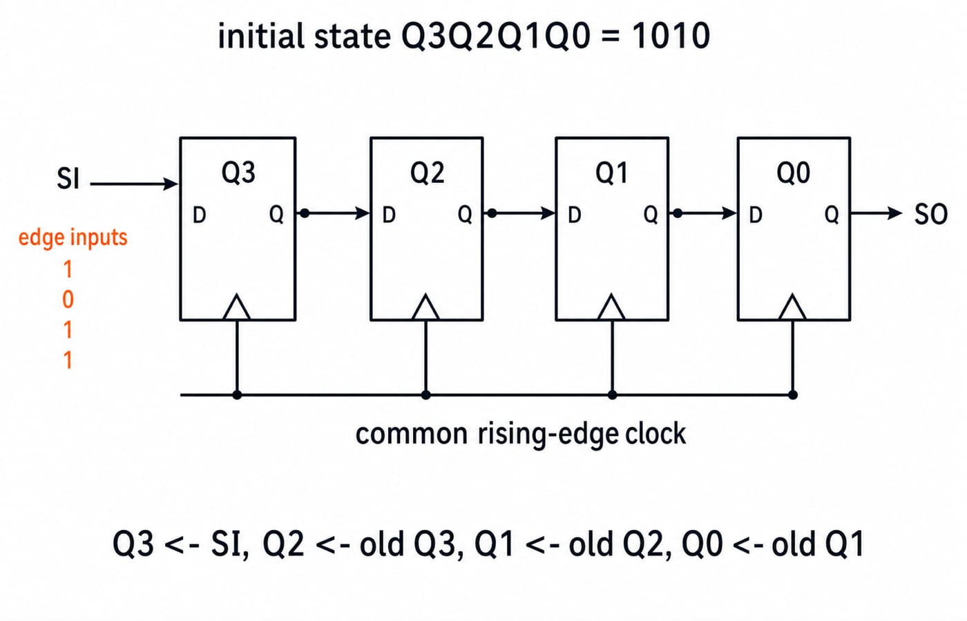
Fix the notation before using the phrase right shift. The state is written as Q3 Q2 Q1 Q0, from the most significant position to the least significant position. A right shift means:
Q3 <- SIQ2 <- old Q3Q1 <- old Q2Q0 <- old Q1
The bit shifted out during the edge is old Q0. Every value on the right is read from the pre-edge state. All four outputs then take their new values after that same edge. This simultaneous-update rule is the key mental model. The CS Fundamentals hub places this idea within the wider digital-logic foundation.
SISO, SIPO, PISO and PIPO describe how data enters and leaves
These four labels describe input and output access. They do not create four different storage laws.
Type | Input | Output | Main behaviour |
|---|---|---|---|
SISO | Serial | Serial | Delays a bit stream through |
SIPO | Serial | Parallel | Converts a serial stream into a word visible across all stages |
PISO | Parallel | Serial | Loads a word together, then emits one bit per active edge |
PIPO | Parallel | Parallel | Loads and reads all bits together like a conventional register |
In every case, each flip-flop holds one bit and the stages share a clock. A practical register can provide several modes through control inputs. The same synchronous-state reasoning applies across all four access patterns.
Order still matters. If a PISO register holds Q3Q2Q1Q0 = 1011 and right-shifts under this convention, its old stored bits leave LSB first: 1, 1, 0, 1.
Worked example: trace a 4-bit right-shift register for four clocks
Take four rising-edge D flip-flops with state order Q3Q2Q1Q0. The initial state before edge 1 is 1010. Apply serial inputs 1, 0, 1, 1 at edges 1 to 4. At each edge, record old Q0 as the shifted-out bit, then apply the right-shift equations simultaneously.
Edge | SI | State before | Shifted-out bit = old Q0 | State after |
|---|---|---|---|---|
1 |
|
|
|
|
2 |
|
|
|
|
3 |
|
|
|
|
4 |
|
|
|
|
At edge 1, old Q0=0 leaves while input 1 enters Q3, producing 1101. Notice that every row's state before is exactly the preceding row's state after. That continuity is a quick way to catch a copied or shifted bit.
Walk through edge 2 carefully. The old state is 1101, so old Q3=1, old Q2=1, old Q1=0, and old Q0=1. With SI=0:
new
Q3=0new
Q2=1new
Q1=1new
Q0=0
The new state is therefore 0110. The newly calculated Q2 must not feed Q1 during this edge. Q1 samples old Q2.
The output column also shows that the initial word 1010 leaves in the order Q0,Q1,Q2,Q3 = 0,1,0,1. After four edges, the register holds the supplied inputs in reverse arrival order: SI4 SI3 SI2 SI1 = 1101.
Read timing, latency and serial order without an off-by-one error
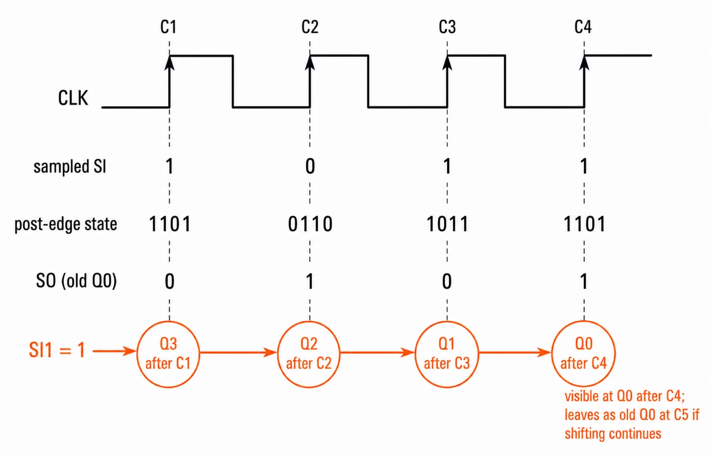
The value visible at Q0 after an edge is different from the old Q0 that leaves during that edge. In the four-clock trace, SI1=1 enters Q3 after edge 1. It moves to Q2 after edge 2, Q1 after edge 3, and Q0 after edge 4. If shifted out means the pre-edge Q0 recorded at each active edge, this inserted bit leaves on edge 5.
In general, an n-stage SIPO register needs n active edges to place n newly supplied serial bits across its parallel outputs. A bit inserted at the first edge reaches the final stage after edge n. Always check whether a question samples before or after the edge. Physical outputs also change after a propagation delay, so keep delay qualitative unless the problem provides a numerical value.
Bidirectional and universal shift registers add controlled next-state choices
A bidirectional register can shift toward either end. With the written order Q3Q2Q1Q0, a left shift uses Q3 <- old Q2, Q2 <- old Q1, Q1 <- old Q0, and Q0 <- SL. Here SL enters from the right.
A universal shift register uses multiplexers before its D inputs to select the source of every next-state bit. The local control table is:
| Selected operation |
|---|---|
| Hold |
| Shift right using |
| Shift left using |
| Parallel load |
This mapping is not universal. A question's supplied selector table always overrides it. Applied independently to the starting state 0110, the four selected operations are:
Mode
00: hold, so0110remains0110.Mode
11,P=1101: parallel load gives1101.Mode
01,SR=0: right shift gives0 0 1 1, or0011.Mode
10,SL=1: left shift gives1 1 0 1, or1101.
How exam-style questions test shift-register reasoning
Stable question forms include finding a state after an input sequence, recovering serial output order from a loaded word, counting conversion edges, choosing a timing trace, deriving D-input equations, and applying a supplied mode-control table.
Try two rapid checks:
Start from
0011. A right shift withSI=1produces1001and shifts out1. A second right shift withSI=0produces0100and shifts out1.Load a right-shifting PISO register with
1011. Its old word emerges LSB first as1,1,0,1over four shifts.
Sequential Circuits MCQs: 11 Solved GATE Questions provides adjacent practice.
Traps that change the answer
Do not assume that right shift explains itself. First write the displayed order, serial-input side, output side, and update equations. A diagram or textbook may place Q0 and Q3 differently.
Do not cascade fresh values through the register within one clock. Edge-triggered flip-flops sample together, so every right-hand side must use an old output. Label serial inputs by edge as well. This prevents you from reversing the sequence or writing the final state in arrival order instead of the requested Q3Q2Q1Q0 order.
Also separate Q0 after edge 4 from old Q0 shifted out at edge 4, and copy the selector table given in the question. If JK or T flip-flops implement the register, convert each required next state through the relevant excitation relation. Flip-Flop Conversion for GATE develops that extension.
The short version and the next practice step
Fix the bit order, write one simultaneous next-state equation per stage, build a pre-edge and post-edge table, and only then read the final state and output. For the stated inputs, the trace is 1010 --SI 1/0--> 1101 --SI 0/1--> 0110 --SI 1/0--> 1011 --SI 1/1--> 1101, with each label written as input/output.
Redo it for inputs 0,1,0,0 and verify every old Q0. GATE-focused learners can follow GATE Guidance by Sanchit Sir, while learners building broader core-CS foundations can use the Zero to Hero Complete CS Course.
Keep learning
NOT, OR and AND Gates: Evolution, Truth Tables and a Worked Circuit
Learn how NOT, OR and AND gates developed from switching ideas, then trace F=(A+B')C node by node and confirm it with a complete truth table.
Updated 23 Oct 20265 min readDigital Logic
Binary Arithmetic Operations Explained: Rules and Worked Examples
Learn binary addition, subtraction, multiplication and division with aligned worked examples, then separate carry, borrow and two's-complement overflow.
Updated 19 Oct 20266 min readDigital Logic
1's Complement Explained: Binary Conversion, Addition and Worked Examples
Learn how fixed-width 1's complement numbers represent negatives, why zero has two encodings, and how end-around carry works through exact examples.
Updated 15 Oct 20266 min readDigital Logic
Decimal Conversion Explained: Binary, Octal and Hexadecimal Worked Examples
Learn one dependable method for converting values between decimal, binary, octal and hexadecimal, including fractions, shortcuts and checks.
Updated 11 Oct 20265 min readDigital Logic