Control Unit Design Cross-Concept MCQs: 12 Solved Questions with Explanations
Solve 12 published Control Unit Design questions covering address capacity, datapath scheduling, DRAM refresh, register widths, bitwise arithmetic and decoding. Each answer shows the decision or calculation that matters.
KnowledgeGate Team
Exam prep & CS education
25 Aug 20267 min read

Cross-concept Control Unit Design questions jump between bus widths, micro-operation ordering, refresh timing and address decoding. Solve all 12 before checking the explanations so that each miss identifies a specific decision rule. CPU Organization Basics MCQs: 12 Solved Questions establishes the address, instruction and register roles needed before tracing cycle overlap, bitwise strength reduction and non-contiguous decoding.
Control Unit Design cross-concept MCQs: choose the right quantity first
Name the tested quantity first; similar widths do different jobs.
Question cue | Quantity or order to compute |
|---|---|
32 address lines, byte-addressable |
|
32 multiplexer inputs |
|
1K DRAM rows |
|
8-line address bus | 8-bit PC |
Single-bus datapath | Fetch, operand staging, ALU work, write-back |
Address, data and instruction widths set location count, transfer width and IR width respectively. For Questions 3, 4 and 7, list destination values before transfers. Pipelining in Computer Architecture: Speedup and Hazards covers dependent CPU stages.
Address-bus capacity and processor-power questions
Question 1: distinguish address width from data width
The maximum addressing capacity of a microprocessor with a 16-bit data bus and a 32-bit address bus isA. 64 K.
B. 4 GB.
C. Both A and B.
D. None of these.B, 4 GB. With byte addressing, 2^32 = 4,294,967,296 byte addresses, or 4 GB. A 16-bit data bus changes transfer width only.
Question 2: identify all three independent processing-power factors
ISRO 2020
Which factors affect processing power, assuming they do not influence one another?
1. Data-bus capability
2. Addressing scheme
3. Clock speedA. 3 only
B. 1 and 3 only
C. 2 and 3 only
D. 1, 2 and 3D, 1, 2 and 3. The items are data-bus capability, addressing scheme and clock speed. Independently, each affects useful work; clock speed alone does not measure real-world CPU performance. Review the processing-power factors question.
Internal forwarding and call-instruction execution cycles
Question 3: forward the register value before writing memory
GATE IT 2004
If we use internal data forwarding to speed up the performance of a CPU (R1, R2 and R3 are registers and M[100] is a memory reference), then the sequence of operations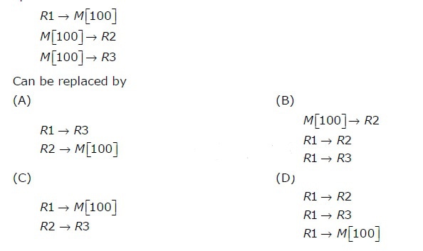
A. A
B. B
C. C
D. D
D. Forward R1 to R2 and R3, then write it once to M[100], preserving destinations without reads. B omits memory; C omits R2.
Question 4: overlap the ALU increment with the memory read
GATE 2005
Consider the following datapath of a CPU. The ALU, bus and all registers in the datapath have identical widths. All operations, including incrementing the PC and GPRs, are carried out in the ALU. A memory read takes two clock cycles: the first loads the address into the MAR, and the second loads data from the memory bus into the MDR.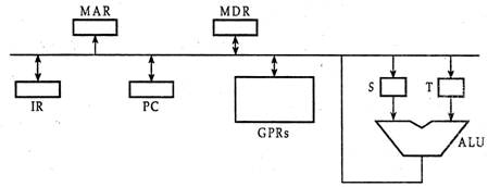
The instruction "call Rn, sub" is a two-word instruction. Assume that the PC is incremented during the fetch cycle of the first word. Its register-transfer interpretation is:
Rn <= PC + 1
PC <= M[PC]
The minimum number of CPU clock cycles needed during its execution cycle is:A. 2
B. 3
C. 4
D. 5B, 3 cycles. Cycle 1 sends PC to MAR and the ALU. Cycle 2 performs memory-to-MDR beside PC + 1-to-Rn; cycle 3 sends MDR to PC. The separate path permits overlap.
Program-control statements and DRAM refresh timing
Question 5: find the one true program-control statement
UGC NET 2021
Which of the following statements is true?
A. Control memory is part of the hardwired control unit.
B. Program-control instructions alter the sequential flow of a program.
C. Register-indirect addressing for a memory operand is similar to displacement addressing.
D. CPU utilisation is not affected by interrupts.A. A
B. B
C. C
D. DB, statement B. Control memory belongs to a microprogrammed unit, so A is false; branches and calls alter flow, so B is true. Register-indirect differs from displacement (C false); interrupts consume CPU work (D false). Review the program-control statements question.
Question 6: refresh 1K rows across all chips in parallel
GATE 2010
A main memory unit with a capacity of 4 megabytes is built using 1M×1-bit DRAM chips. Each DRAM chip has 1K rows of cells with 1K cells in each row. The time taken for a single refresh operation is 100 nanoseconds. The time required to perform one refresh operation on all the cells in the memory unit isA. 100 nanoseconds
B. 100×2^10 nanoseconds
C. 100×2^20 nanoseconds
D. 3200×2^20 nanosecondsB, 100×2^10 nanoseconds. One command refreshes a row across all chips, so multiply by neither chips nor cells. 1K = 2^10 = 1024 rows, hence 1024 × 100 ns = 102,400 ns = 102.4 microseconds. Cache Memory Mapping and Hit Ratio: Solved Examples covers a different mechanism.
Datapath ordering and multiplexer select-line questions
Question 7: order fetch, operand staging, ALU work and write-back
GATE 2020
Consider the following data path diagram.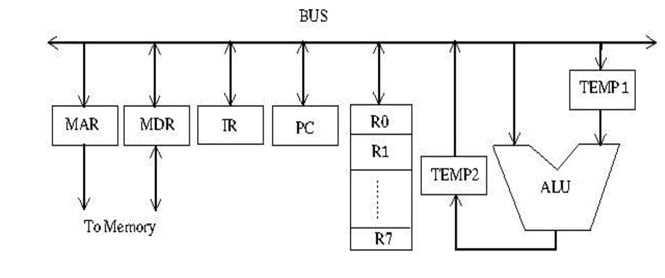
Consider the instruction \(R0 ← R1 + R2\). The following steps execute it over the datapath. Assume that the PC is incremented appropriately. Subscripts r and w indicate read and write operations.
1. \(R2_{r}, \text{TEMP1}_{r}, ALU_{\text{add}}, \text{TEMP2}_{w}\)
2. \(R1_{r}, \text{TEMP1}_{w}\)
3. \(PC_{r}, \text{MAR}_{w}, \text{MEM}_{r}\)
4. \(\text{TEMP2}_{r}, \text{R0}_{w}\)
5. \(\text{MDR}_{r}, \text{IR}_{w}\)
Which option gives the correct execution order?A. 2, 1, 4, 5, 3
B. 1, 2, 4, 3, 5
C. 3, 5, 2, 1, 4
D. 3, 5, 1, 2, 4C, 3, 5, 2, 1, 4. Fetch is 3 (PC to MAR) then 5 (MDR to IR). Next stage R1 (2), produce TEMP2 (1), then write R0 (4): 3 -> 5 -> 2 -> 1 -> 4.
Question 8: compute select lines from the register count
GATE 2020
A multiplexer is placed between a group of 32 registers and an accumulator to regulate data movement such that at any given point in time the content of only one register will move to the accumulator. The number of select lines needed for the multiplexer is _________ .5. With s lines, a multiplexer selects 2^s inputs. Since 32 = 2^5, s = 5; four lines cover 16 inputs, while six are unnecessary.
CPU register widths and address-storage questions
Question 9: test the absolute word never
Which of the following CPU register will never be storing any memory address?A. Program counter
B. Stack pointer
C. Memory data register
D. NoneD, None. PC and stack pointer normally hold addresses. An MDR word can also be an address, though that is not its dedicated role, so never fits none.
Question 10: derive IR, MBR, PC and SP widths independently
Consider a computer system which uses a memory with 8-address lines and 16-data lines. The instructions used in the system are of 32bits. Which of the following is/are correct?A. CPU has instruction register size 32-bit.
B. CPU has memory buffer register size 16-bit
C. CPU has program counter size 8-bit.
D. CPU has stack pointer size 16-bitA, B and C. Instruction, data and address widths set IR, MBR and PC to 32, 16 and 8 bits. The stack pointer holds an 8-bit address, not 16-bit data, so D is false.
Bitwise strength reduction and non-contiguous address decoding
Question 11: replace modulo 64 and multiplication by 5
Your code must compute (A % 64) * 5. Which replacement eliminates multiplication (*) and modulo (%), assuming A is 32 bits wide?A. Shift A right by 6, shift left by 2, and add the current value to itself.
B. Shift A right by 6, save the result, and add the saved result to the current result once.
C. AND A with 0000003F, save the result, and add the saved result to the current result twice.
D. AND A with 0000003F, save the result, shift the result left by 2, and add the saved result to the current result.D. Because 64 = 2^6, set x = A & 0x0000003F, then 5x = (x << 2) + x. At A = 77, x = 13, x << 2 = 52, and 52 + 13 = 65 = (77 % 64) × 5.
Question 12: decode IA4 and IA3 into the four block starts
GATE 2023
A 4 kilobyte (KB) byte-addressable memory is realized using four 1 KB memory blocks. Two input address lines (IA4 and IA3) are connected to the chip select (CS) port of these memory blocks through a decoder as shown in the figure. The remaining ten input address lines from IA11–IA0 are connected to the address port of these blocks. The chip select (CS) is active high.The input memory addresses (IA11–IA0), in decimal, for the starting locations (Addr=0) of each block (indicated as X1, X2, X3, X4 in the figure) are among the options given below. Which one of the following options is CORRECT?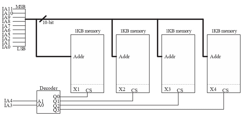
A. (0, 1, 2, 3)
B. (0, 1024, 2048, 3072)
C. (0, 8, 16, 24)
D. (0, 0, 0, 0)
C, (0, 8, 16, 24). Local inputs are 0 at each block start. Decoder bits IA4 IA3 run 00, 01, 10, 11; weights 16 and 8 give 0, 8, 16, 24. Option B needs unshown highest bits.
Control Unit Design MCQs: diagnose the miss and choose the next drill
Misses on Questions 1, 2 or 10 mean width roles are mixed. For Questions 3, 4 or 7, write the micro-operation schedule; for 6, 8 or 12, revise powers of two and bit positions; for 11, practise masking and shift-add identities.
Redo Questions 4, 7, 11 and 12 without answers to practise cycle overlap, dependency order, arithmetic transformation and decoding. Use GATE Guidance by Sanchit Sir for a structured COA sequence, or GATE CS Exam Preparation for the wider catalogue.
Keep learning

Data Manipulation Micro-Operations MCQs: 10 Solved Questions with Explanations
Solve 10 micro-operations MCQs with step-by-step explanations of shifts, ALU behaviour, register logic, Booth recoding and control width.
Updated 20 Oct 20267 min readComputer Organization MCQs

Performance & Speedup MCQs: 12 Solved Pipelining Questions
Work through 12 solved pipelining questions step by step, from finite pipeline time and latch overhead to bubbles, MIPS, CPI and bottleneck splitting.
Updated 16 Oct 20268 min readComputer Organization MCQs

Multiprocessor Classification MCQs: 8 Solved MCQs and 2 Concept Checks
Work through the complete mapped pool: eight objective items plus two optionless concept checks. Explanations cover Flynn's taxonomy, coupling, bus facts, and parallel efficiency.
12 Oct 20267 min readComputer Organization MCQs

Input Output Organisation MCQs: 12 Cross-Concept COA Questions Solved
Test 12 Input Output Organisation MCQs across storage, spooling, I/O instructions, interrupts, DMA, arbitration and bus bandwidth.
8 Oct 20268 min readComputer Organization MCQs